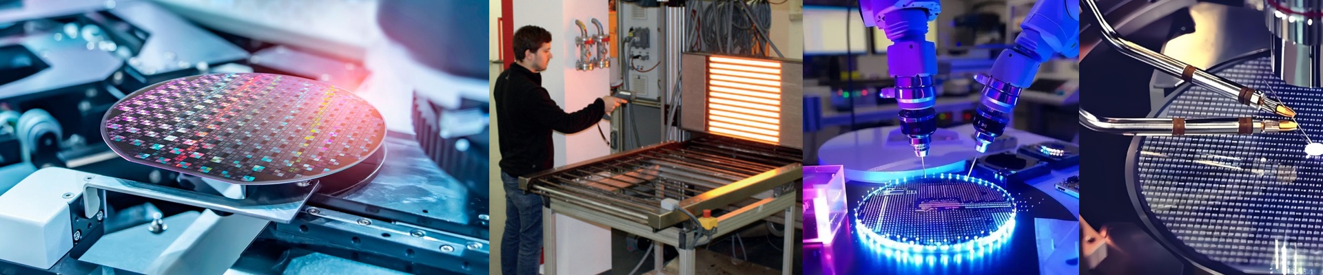

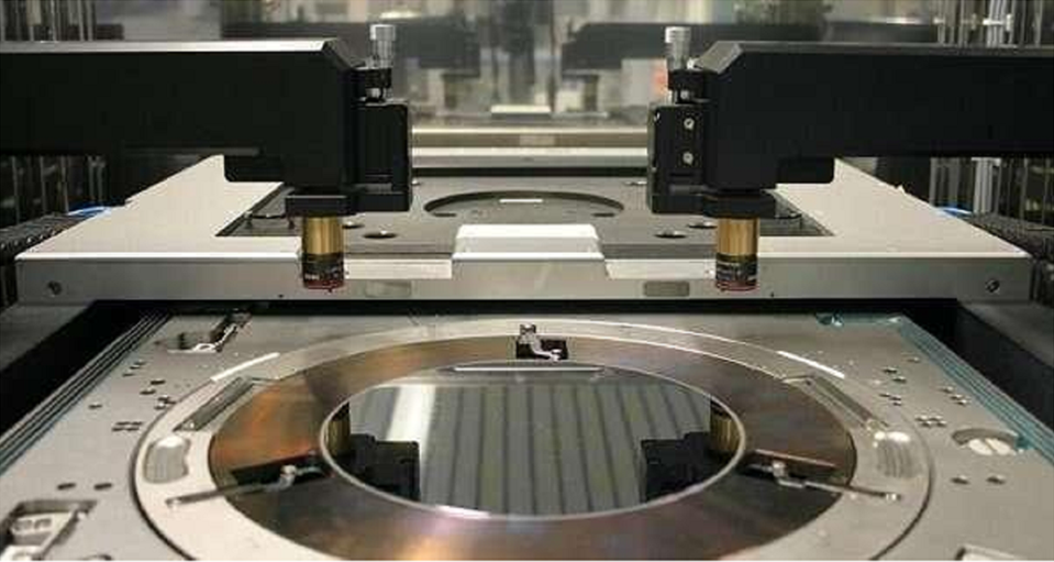
On the fab floor, temperature isn’t just a parameter. It is the process. A bake temperature drift will move photoresist flow and shift critical dimension. A hot spot during wafer drying can create a micro-skin and turn the surface into a particle trap. In packaging, a cure profile that isn’t uniform shows up as warpage and delamination—often only after singulation, when the die is already paid for. When thermal control misses, the line doesn’t just slow down. Yield and repeatability go first. We built infrared heating modules for the fab because thermal control has to be measurable, stable, and clean enough to live inside Class 1–100 environments—without adding risk to the process chamber.
What actually matters, technically
Infrared heating in semiconductor work comes down to three things: wavelength choice, temperature control, and clean operation. We match short-wave and medium-wave infrared sources to how silicon, quartz, and polymer films absorb, so we heat fast and direct without hauling around a lot of extra thermal mass. The modules are engineered for wafer-level thermal uniformity of ±0.1°C, because lithography and photoresist bake budgets are written in that kind of tolerance. Temperature repeatability is held tight so the thermal history is the same shot-to-shot, wafer-to-wafer. The hardware is specced for 24/7 running: stable output over thousands of hours, predictable maintenance intervals, and consistent performance after each lamp replacement cycle. In the cleanroom, particle generation is controlled by design—no exposed hot filaments, no outgassing-prone materials in the beam path, and surfaces that don’t shed. The payoff is heating that keeps chamber particle counts down, not just on the report, but across shifts. Power, voltage, and footprint are matched to retrofit needs and OEM integration. Output is tuned through closed-loop control, so the module responds to real temperature feedback instead of running open-loop and hoping the setpoint lands.
Why it fits where the fab uses heat
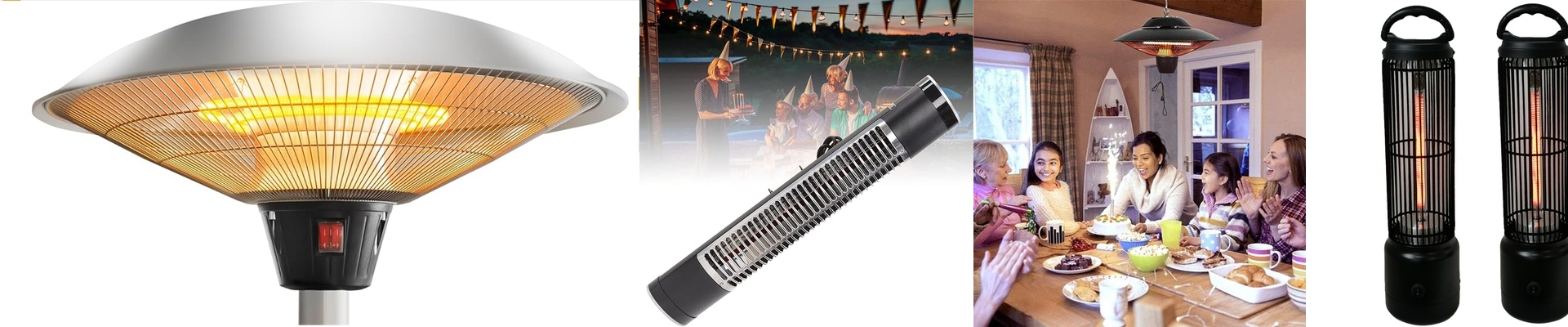
The fab uses heat in four places where precision isn’t optional: wafer drying, photoresist baking, packaging curing, and cleaning/drying. In each, the infrared module earns its keep by cutting out the usual compromises. Wafer drying after wet cleaning is where surface tension collides with thermal physics. Conventional hotplates can leave a thermal gradient across the wafer, and that gradient shows up as uneven drying—water marks, streaks, and edge residues. Infrared heating dries from the top surface downward, delivering controlled energy that lowers the risk of skin formation. Hit the uniformity target, and the whole wafer behaves the same way, so drying stops being a quiet yield killer. Photoresist processing—soft bake and hard bake—lives or dies on temperature accuracy. Too cold, and solvents hang around. Too hot, and the resist flows, changing critical dimensions and sidewall angles. Infrared modules give you fast ramp-to-setpoint response and a stable hold at the bake temperature, which tightens photoresist profile control and cuts within-batch variation. That translates straight into tighter CD control and fewer excursions you can trace back to the bake step. Packaging curing demands throughput without cutting corners on reliability. B-stage materials and underfills need a thermal profile that repeats across thousands of units. Infrared provides rapid, localized heating that shortens cycle time while keeping the thermal budget controlled. Uniform cure across the substrate reduces warpage risk and improves reliability in temperature cycling. Cleaning and drying—whether solvent or aqueous—always ends with a dry-down that has to be residue-free. Infrared drying cuts carryover by driving off residual liquids quickly and evenly, which supports lower defect counts and more consistent surface prep before the next thin-film step. Across these applications, the gains are practical: stable process windows, fewer rework lots, and maintenance you can plan. Energy use also improves because infrared puts energy where it’s needed, when it’s needed, instead of heating an entire platen and waiting.
What you need to know before you spec it
Infrared heating is straightforward to integrate, but it isn’t plug-and-play without planning. Integration means paying attention to optical path clearance, shielding, and thermal isolation. Mount the module so reflected energy doesn’t couple into adjacent sensors, mechanical stages, or polymer parts. If your chamber has tight vertical clearance, treat the beam profile and mounting hardware as one spec, not an afterthought. Process compatibility depends on picking the right wavelength and power density. Some polymer stacks and thin-film stacks absorb differently across the infrared spectrum, so what works for one stack can be suboptimal for another. We size the module and tune the control strategy to the substrate’s thermal mass and absorption behavior, not just the nominal setpoint. Maintenance is real, not theoretical. Lamps and optics have finite life. Plan replacement cycles and keep spares on the shelf. The upside is predictability: performance degrades gradually, not suddenly, so you can schedule maintenance around planned downtime. And here’s the part that bites if you ignore it: infrared heating is sensitive to emissivity differences across materials. Change films, substrates, or even wafer backside conditions, and the absorbed energy changes. That’s not a flaw—it’s a parameter. Calibrate the recipe once, then lock it into the control method. Do that, and the module behaves like a fixed process constant instead of a variable you chase. If your line is running at wafer-level precision, the heating system has to be part of the process spec, not an external dependency. Infrared modules deliver that control—clean, repeatable, and measurable—where the fab needs it most.