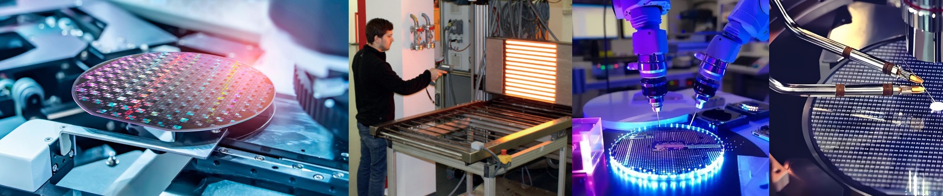
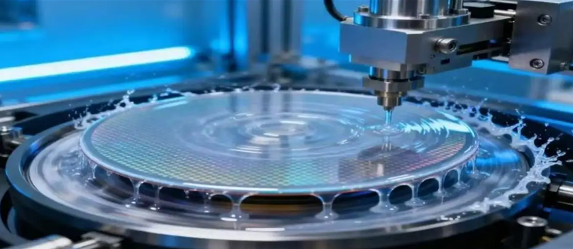
On the fab floor, a wet wafer is a liability you can’t afford. Leftover moisture sets you up for pattern collapse after exposure, and a bake profile that’s even slightly off will drift your critical dimensions. That’s why the solar cell wafer drying lamp exists: to take the guesswork out of wafer drying, photoresist soft bake and hard bake, packaging encapsulation cure, and post-clean drying. We built the lamp around near-infrared (NIR) halogen emitters in a quartz assembly. The point is rapid, directional heating with low thermal mass. That translates to fast settling and tight control: ±0.1°C wafer-level uniformity across the illuminated zone, repeatable setpoint-to-wafer response, and cleanroom-compatible construction for Class 1–100. Output stays stable over long runs, too. Field units have logged 5,000+ hours with less than 5% intensity drift. And we keep particle generation low with a sealed optical path and low-outgas materials, so contamination stays out of the process chamber. In lithography, the lamp dries wafers fast without solvent streaks, then runs soft bake and hard bake at stable temperatures that protect CD and profile targets. In packaging, it speeds up encapsulant cure without blowing the substrate thermal budget. After wet cleaning, it dries patterned wafers clean—no watermarks—so you cut rework. Energy use is managed by duty-cycled heating and efficient coupling into the wafer, so you keep throughput while operating costs come down. Installation comes down to details. Get the optical alignment right and make sure the lamp housing has adequate exhaust; thermal coupling shifts if the distance varies by even a few millimeters. The lamp performs best on flat, reflective, or dark surfaces. Highly textured or uneven substrates will move local temperature, so plan your fixture to match the wafer path. Verify voltage and connector specs against your tool.With the setup dialed in, you widen the process window and shave cycle time—without giving up yield.