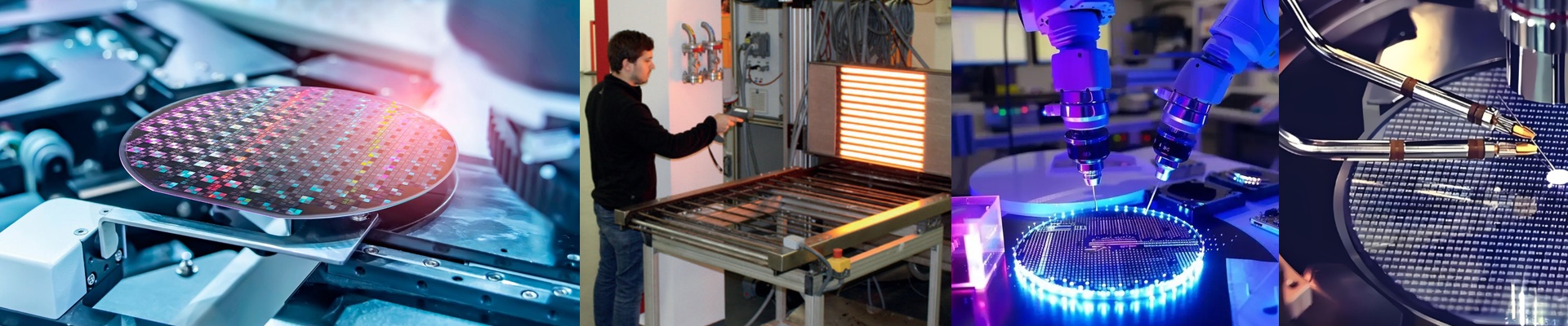
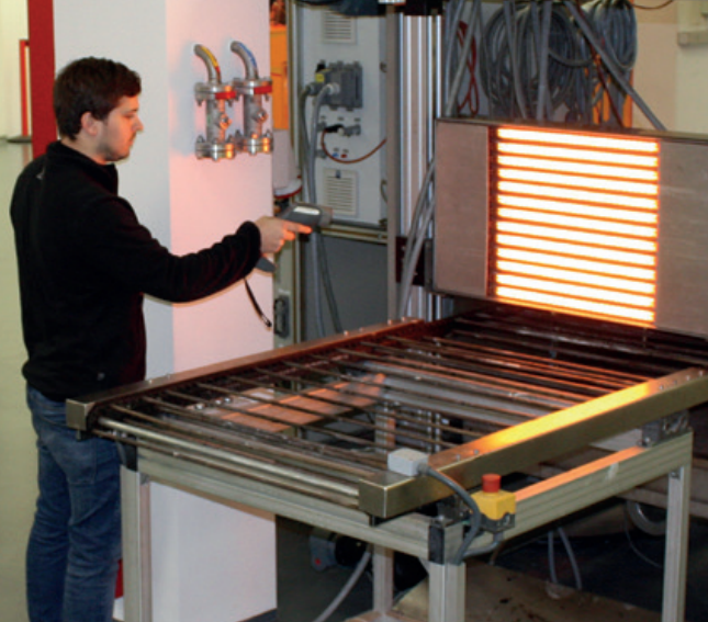
On the 300mm line, glue cure isn’t just another thermal step. It’s a dimensional constraint. A few degrees of drift and the photoresist profile moves, overlay starts to slip, and yield dips before the reticle even hits the wafer. That’s why we moved to infrared for semiconductor glue—to pull the variability out of the equation. What matters under the hood We hit the adhesive and photoresist layers with near-infrared (NIR) tuned for rapid, volumetric heating. The payoff is wafer-level temperature uniformity within ±0.1°C across the shot, measured at the film interface, not some heater surface. The tool lives in the cleanroom without drama—Class 1–100 operation, zero particle generation, verified by in-situ particle monitoring. It runs repeatable soft bake and hard bake profiles with tight thermal budget control, and it holds up in high-volume lines, 24/7, with no unplanned downtime. Why it fits the process In lithography and bonding, you need heat where it matters—in the film, not the carrier. NIR delivers energy immediately and on target, which shortens cycle time without blowing critical dimensions. Tight uniformity keeps edge devices in spec and cuts scrap. Power use drops because the heat is absorbed directly, not dumped into chamber mass. And repeatability makes qualification cleaner, control limits tighter, and rework far less frequent. Here are the realities on the floor NIR needs direct line-of-sight and controlled emissivity on the wafer backside. If the carrier is reflective or textured, you’ll scatter energy and shift the profile. Expect a short integration window to line up the thermal profile with the specific glue stack and substrate stack-up. Once you get it dialed, the process window hardens, and the line settles—no more noise from thermal variation.