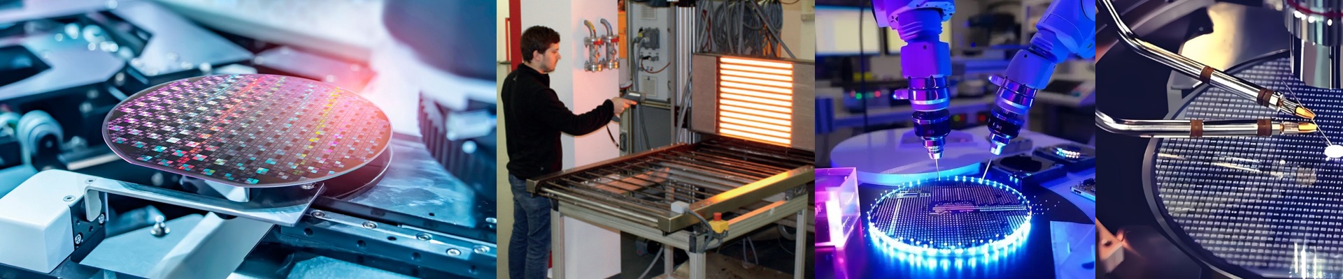
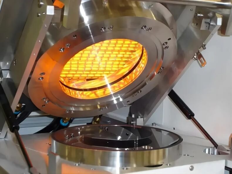
On the wafer floor, a half-degree drift during drying is enough to throw off critical dimension bias and start throwing resist defects. You need heat that hits exactly what the process card calls for, shift after shift, lot after lot. That’s the reality these silicon wafer drying infrared lamps are built around. What matters, technically We run short-wave infrared emitters with fast ramp-up and tight spectral control, so you get quick thermal transfer without blowing past the photoresist thermal budget. Across the illuminated zone, wafer-level uniformity stays within ±0.1°C, and repeatability is nailed down by closed-loop pyrometry right at the lamp exit. The whole system is cleanroom-compatible from Class 1 to Class 100, with materials and housing geometry that keep particle generation effectively flat. In the field, units have racked up 5,000+ hours and still hold output stability within 5%—the kind of uptime you can count on. Why it holds up in real processes In spin-rinse drying and post-clean moisture removal, the infrared profile dries wafers faster while staying off pattern collapse and edge bead issues. In lithography, the same lamps cover soft bake and hard bake with temperature control that’s actually repeatable, so line-width control tightens up and rework drops. The payoff is fewer scrap lots, lower energy draw thanks to efficient radiant coupling, and less downtime spent on maintenance. The design meets international semiconductor equipment expectations and gives you a validated, equivalent alternative for existing platforms. Here’s what you need to plan for Installation comes down to thermal clearances and airflow—mount the lamp to the specified standoff and align it to the wafer path, or you’ll lose the uniformity you’re after. Electromagnetic compatibility near scanners and track units may require shielding or routing adjustments. Plan a short commissioning run to map temperature profiles against your process recipe, then lock the setpoints in place.